High frequency WBG of cascode GaN/SiC
10/29/2022 11:00:08 AM
As the demand for smaller and more efficient electronic systems continues to surge, engineers have been exploring different topologies and semiconductor technologies. By increasing the switching frequency, engineers have successfully reduced energy storage in passive components, leading to more compact systems. WBG power devices offer superior advantages over traditional silicon-based components, making them crucial elements in the modern power electronics industry.
GaN devices, particularly lateral GaN High Electron Mobility Transistors (HEMTs), have proven to be highly suitable for high-frequency applications and low-voltage scenarios. However, limitations in voltage ratings and Coss losses under Zero-voltage switching (ZVS) conditions have been challenging. On the other hand, SiC devices, known for their impressive voltage ratings and low conduction losses, are predominantly used in higher voltage and lower frequency applications. Although SiC devices possess large gate charges, recent research suggests their potential to outperform GaN devices at high frequencies and low currents. Understanding the distinct characteristics of GaN and SiC devices holds the key to designing more efficient and compact electronic systems, which help in the research of high-frequency and high-power converters.
Cascode GaN/SiC Power Systems
The cascode GaN/SiC power device combines a depletion-mode 1200 V SiC JFET and an enhancement-mode 100 V GaN HEMT. SiC JFET offers stable threshold voltage, while GaN HEMT provides a moderate voltage rating, low on-resistance, and small gate charge. The devices are connected in a cascode configuration, allowing easy high-frequency driving with a comparable voltage blocking to SiC JFET.
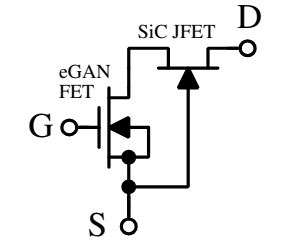
Fig 1: Cascode GaN/SiC power device schematic diagram
A. Switching Sequence of Cascode GaN/SiC Device: In Figure 2, the Class E inverter's cascode GaN/SiC device exhibits a specific switching sequence. Reducing gate losses can be achieved by adding external capacitors in parallel to the SiC JFET. However, this comes at the cost of an increased maximum drain voltage for the GaN FET. Careful consideration is necessary as it may impact the overall performance and reliability of the system. Balancing these factors is crucial when optimizing the inverter's design for efficiency and robustness.
.png)
Fig 2: Switching sequence with hard and soft turn-on time.
B. Analyzing SiC JFET Gate Loss in Cascode GaN/SiC Devices: Gate loss in SiC devices is typically high in HF/VHF circuits due to gate charge and voltage. However, cascode GaN/SiC devices offer zero gate loss in soft-switching with minimal Rg, Jfet. Turn-off charges Coss of GaN FET and SiC JFET capacitors by ID. In a soft-switching scenario, SiC JFET gating loss can be eliminated; in hard-switching, it can be reduced by half. Fig 3 shows the turn-on process of the GaN FET and all of the SiC JFET capacitors.
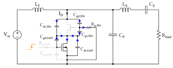
Fig 3: Cascode GaN/SiC device's turn-on behavior in a Class E inverter schematics.
C. Energy Loss of Small Signal Coss and Large Signal Coss : The small signal Coss of the cascode GaN/SiC device was measured using an impedance analyzer from 0 V to 560 V at 1 MHz. When the DC drain voltage is below -Vth,Jfet, Coss is similar to GaN FET. Above -Vth,Jfet, most voltage is blocked by SiC JFET, making Coss a combination of Coss,Jfet and Coss,GaN. At 500 V, the measured Coss is 40 pF with Vds,GaN ranging from 7 V to 17 V.
Studying SiC Mosfet, SiC JFET and Cascode GaN/SiC Device in a Class E inverter and their Advantages
The researchers compared a cascode GaN/SiC device and SiC MOSFET and SiC JFET in Class E inverters. The cascode device showcased several advantages over individual SiC devices. Firstly, it exhibited a higher breakdown voltage of 1350 V, providing increased robustness for high-power applications. Secondly, the cascode configuration led to a simpler and smaller auxiliary gate drive circuit since the SiC JFET in the cascode device could draw its gating power from the circuit's main supply. As a result, the gate driver only required driving the GaN FET, reducing complexity and board space requirements. Figure 4 shows the performance of the drain voltage and gate-to-source voltage Vgs(t) of the SiC JFET in the cascode.
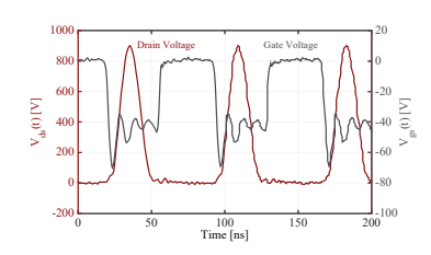
Fig 4: Waveform of the drain voltage and gate-to-source voltage in the SiC JFET in the cascode device.
In contrast, using the SiC JFET alone demanded a higher-power gate driver and a separate isolated DC-DC converter was needed to supply the negative gate voltage. The gate drive circuit for the cascode GaN/SiC device proved to be the simplest among the three, requiring less than 1 W from a 5 V gate driver, while the SiC MOSFET and SiC JFET needed 40 W from a 20 V gate driver and 20 W from a -20 V gate driver, respectively. Overall, the cascode GaN/SiC device's advantages in breakdown voltage and gate drive circuit simplicity make it an attractive option for power electronics applications, especially where high-voltage capabilities and efficient gate driver design are essential considerations.
The integration of cascode GaN/SiC power devices offers several advantages over traditional GaN-on-Si devices. SiC has a lower lattice and thermal expansion mismatch with GaN, resulting in smaller Coss losses and higher drain current ratings. Additionally, SiC's higher thermal conductivity facilitates better heat dissipation. Integrating the cascode device reduces parasitics, enables smaller Rds,ON, and minimizes SiC JFET gate power loss. The integration also allows for a reduction in gate resistance by redesigning the device structure and the p+ gate region. These improvements make the cascode GaN/SiC device a promising option for power applications.
Conclusion
Researchers compared the performance of Class E inverters comprosing of SiC MOSFET, SiC JFET, cascode GaN/SiC device. Cascode achieved highest efficiency, simpler, cheaper, smaller drive circuit. As a future scope integration of cascode GaN/SiC for high-frequency and high-power circuits can be done for further investigation
Blog Category
NewsLatest Products
-
IP5002CX8/P135
NXP USA Inc.
-
ADAU7002ACBZ-RL
Analog Devices Inc.
-
PGA2320IDW
Texas Instruments

-
SRC4184IPAG
Texas Instruments
-
MUSES72320V-TE2
Nisshinbo Micro Devices Inc.
-
PCM2706CPJT
Texas Instruments
-
ZL38040LDG1
Microchip Technology

-
PGA2310UA/1K
Texas Instruments

- Help you to save your cost and time.

- Reliable package for your goods.

- Fast Reliable Delivery to save time.

- Quality premium after-sale service.
-
Tel
+86 14706745934


